FUSION: In-situ
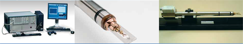
In-situ plasma monitoring system (Wise Probe)
- Measures electron temperature and ion flux during etching in real time
- Can be used as an endpoint detector
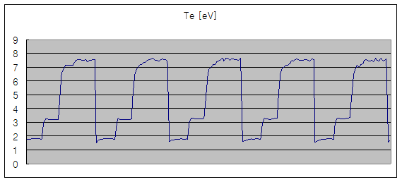
Example of In-situ plasma monitoring
- Electron temperatures of plasma for deep Si etching is measured during the etching.
- Etching with periodic changes in Te (without clear distinction of deposition and etch steps) shows smooth sidewalls (left).
- Etching with clear steps of Te for deposition and etch steps develops scallops (right).


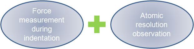
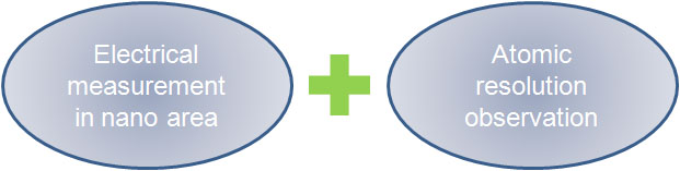
Materials characterization techniques for nano technology, such as AFM, STM, and indentation, are installed in TEM. Mechanical and electrical properties of materials can be measured with atomic resolution image. These novel approaches enable us to understand properties of nano materials correlated with their fundamental atomic structure.

Application 1
Phase change Random Access Memory (PRAM) : PRAM is expected for the next generation
memory device. Switching behavior between crystalline phase (“1” state) and amorphous phase (“0” state) was directly observed with high resolution image.
Application 2
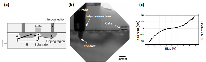
Electrical property mapping : P-N junction identification and dopants mapping in an operating transistor.